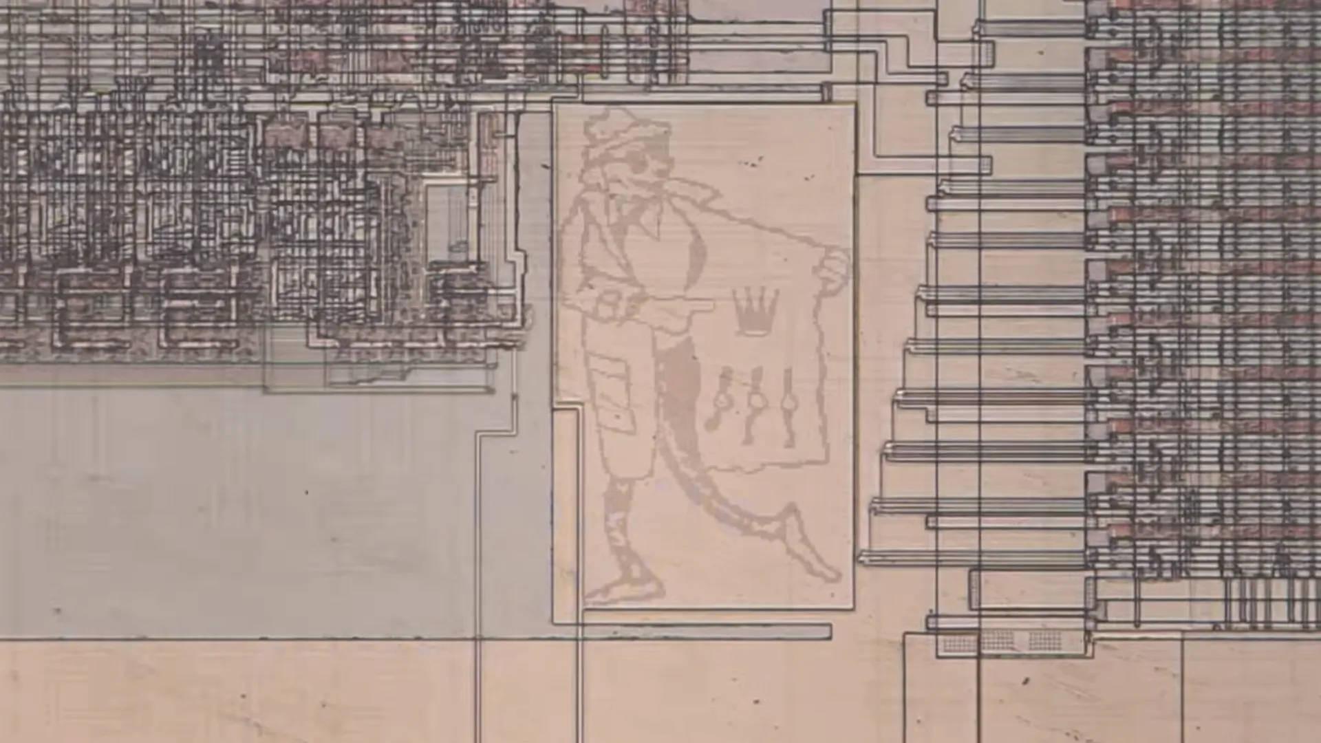
Remember the story from last week about the image of a revolver and map of Texas, etched into one of the layers in AMD’s old K7 chips? Not surprisingly, it isn’t an isolated example of silicon shenanigans, as uncovered by a fan of chip easter eggs shows in an awesome compilation of processors, controllers, and memory die shots. Ducks, zombies, sharks, and dragons rub shoulders with the Playboy logo and a guitar-playing T-rex.
With fewer than 300 subscribers, YouTube channel CPU Duke is unfortunately not likely to appear in your recommended list, but it really should be (thanks to ComputerBase for the heads up). The main reason is the user’s fantastic compilation of old chips being viewed under a microscope, highlighting the neat little easter eggs numerous designers added to the layout.
It’s common practice for manufacturers to add a name or trademark and year to a chip, usually tucked away in a tiny blank section that’s not used in any way. But give an engineer the opportunity to mark their work for prosperity and you’ll get things like we saw with the AMD K7 CPU: an image of a revolver and a map of Texas, the home state of AMD.
But as you can see in the above video, chip designers are often wildly more creative than this. Cue a range of animals, monsters, buildings, and more besides. It has to be said that the quality of images varies a lot but some of these are on really old chips, where the process node technology was nowhere near as precise and near-flawless as it is today.
(Image credit: Future)
Best CPU for gaming: The top chips from Intel and AMD.
Best gaming motherboard: The right boards.
Best graphics card: Your perfect pixel-pusher awaits.
Best SSD for gaming: Get into the game ahead of the rest.
You might be wondering if there’s anything like this on the latest processors from AMD, Intel, Nvidia, et al but I suspect not. The reason for this is the amount of free die space is incredibly small, as today’s chips are designed to minimise the amount of wasted silicon as much as possible.
There could well be some hidden treats tucked away in a remote corner but it might be too small to easily detect in a normal microscope. Unless you’ve got something really powerful to handle and a couple of spare days in which to track across every micron of the die, the chances are that it may be missed for years.
I wonder if I can start a crowdsourced funding project to get my own electron microscope or maybe ‘borrow’ a couple of photomasks from AMD to see if it’s still trying its hand at atomic-level art?


