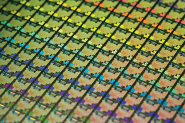
TSMC takes ‘chip binning’ to a whole new level as entire wafer ‘found in a dumpster’
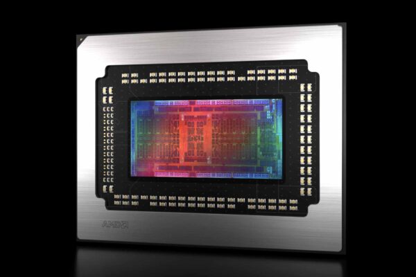
Found this in a dumpster near TSMC fab, how to cut this into usable GPU? from r/pcmasterrace ‘Chip binning’ is supposed to be the process of testing newly manufactured silicon to see how many of the important bits work and how high the thing will clock. But TSMC seems to be taking the notion a…